For a long time, I've wanted to make PCBs at home.
In the past, I used to make my own electronics project using
stripboard and
perfboard. This is reliable, if not slow. But a stripboard design doesn't really lend itself to being constructed by others.
In the past year I've started working with surface mounted devices. SMD doesn't work very well on stripboard, so it becomes not just desirable but necessary to make PCBs. I have put off learning how to do it for a long time, but a month or so ago, I finally got the time to give it a go. This article covers what I currently do, and I'm writing about it here in the hope it will help others.
There are three main ways of making circuit boards at home. The first is via the “toner transfer” method. I have
tried that in the past, but never been able to reliably make a circuit board greater than about a square inch: I've always had a lot of trouble getting the toner 100% fused to the PCB without cracking or smudging.
The second is by using a CNC mill to mill away undesired copper, leaving copper tracks. With the imminent completion of the CNC mill at our hackerspace, or if I one day build a CNC mill using components salvaged from old DVD drives, that might be a possibility. However for the moment I don't have access to a CNC mill, so I can't use that method.
The third is the photographic method. With this method, a special copper-clad PCB is covered by a film of UV-sensitive dye. Exposing the dye to ultraviolet light through artwork printed on transparent paper will leave some regions of dye exposed, and some regions unexposed. A developer chemical will remove the exposed areas, leaving the dye in the form of green tracks on the board. Then the board is etched in a chemical etchant, which removes the copper which is
not protected by the dye. Finally, the dye is removed, leaving copper tracks.
In this article I'll show how to use the photographic method, although I might try the toner transfer and CNC methods again in the future.
The UV-sensitive PCB stock I'm using is sold by
Kinsten, and is available in single- and doubled-sided variants. Here is the Kinsten PCB, plus the developer (Kinsten DP-50), etchant (ammonium persulphate), and a scrubbing pad:
 |
| Kinsten, etchant, developer and scrubber |
In order to generate the UV light, I made an exposer box using nearly 100 UV LEDs. For an enclosure, I cut up and resized a cardboard box. The box is lined with aluminium foil to reflect light towards the board I'm exposing, and the light has to travel through two diffusers of transparent paper.
Here's a picture of the LED array:
 |
| Exposer's UV array, LED side |
And here's a picture of how I wired up the LEDs:
 |
| Exposer's UV array, wiring side |
(The two halves are wired differently because the second board is somewhat smaller than the first board, and wouldn't allow the straight-forward row-and-column arrangement I used on the first board).
The specifications for the LEDs say the forward voltage is about 3V. The wiring of the boards configures the LEDs into many parallel strings of four LEDs. I power the exposer with a 12V power supply. I have adjusted the trimpot on the power supply to get a voltage that gives me a current of 25mA through each LED. The LEDs do get quite warm after running for a while. Here's a picture of the exposer working:
 |
| Exposer powered up showing UV |
NOTE: The LEDs produce a bluish-purple light, but this is not ultraviolet, it's a consequence of the spectrum from the LEDs being spread out somewhat. Our eyes cannot perceive ultraviolet light, yet it is harmful to our eyes. If you are working with ultraviolet light, try to limit how much UV gets into your eyes, or you may have to bear gritty and sore eyes for a few days. UV filtering sunglasses might be a good idea.
I print the artwork for the board on tracing paper I bought from the newsagent. I print it with a laser printer, and in the printer settings dialog I set the density to be as dark as possible. I usually print right-way-around on normal paper to verify that all the parts fit the board, then I print on the transparency
in reverse. If I used a normal printout, there'd be a layer of transparency between the toner and the dye. This can cause blurring, as the UV light can diffuse to under the artwork. Mirroring the image means the toner can be right up against the dye.
 |
| Tracing paper with artwork |
A few weeks ago when I first started this exercise, I didn't know how long to do the UV exposure for. I made some board artwork of ten TQFP-32 footprints in a row, with some lines of different thicknesses. I put the artwork and the PCB on the exposer with a piece of cardboard. Every fifteen seconds I slid the cardboard across by one TQFP, so that by the time two minutes and thirty seconds had elapsed, I had a row of footprints that had been exposed for various times, from 0:15 to 2:30. When I later developed the exposed PCB, what I found was that for my exposer, no pattern emerged until an exposure time of 2:00, and by 2:30 the pattern had developed very nicely. I have since made PCBs with exposure times of 3:00 to 3:30, and they have turned out very nicely.
Some people I've spoken to said I wouldn't be able to reliably make the 0.016” tracks I was hoping for. The good news is that tracks down to 0.010” come out just perfectly, and tracks down to 0.008” (0.2mm) appear very achievable. I think the biggest limiting factor is the quality of the artwork: I can trace small irregularities in the finished PCB to slight imperfections in the artwork, either because of dust or because there is a small hole in the toner. It seems that the toner binds to some places on the transparency better than others.
When doing the exposure, you need some way to keep the artwork flat against the PCB. I use a glass-topped coffee table. I tape the exposer to the bottom side of the coffee table, and put the artwork and PCB on top, held down by a heavy book. I always clean the glass with glass cleaner before doing the exposure.
The dye on the Kinsten PCB is protected by a white plastic film. Just before exposing, I peel off the film, revealing the blue-green dye. I do the exposing well away from the window, as otherwise ultraviolet from the sun may spoil the exposure.
I don't have a picture of a PCB being exposed, because when I'm doing the exposure, I have my hands full with holding the exposer and watching the exposure time.
At the end of the exposure time, I cover the PCB to prevent stray UV light from damaging the exposure. If you look carefully, you should be able to see the pattern of tracks as a very faint yellow hue on the blue-green dye. If you can't see it, it might indicate an exposure problem.
Here I'm developing the board in developer solution:
 |
| Developing Playpause boards in developer solution |
This is 15g of Kinsten DP-50 developer, in 250ml of water. The developer doesn't have to be hot or warm, but having it warm speeds things up a little. While exposing the boards, I rock the container from side to side. As the exposed dye comes off, it makes patterns in the water like smoke.
Here are the boards after they have been developed. I wash them in water, then dry them, being careful not to scratch the ink.
 |
| Developed boards |
Now it's time to etch the boards. There are three main chemicals hobbyists use to etch boards. In order of how often they're used, they are ferric chloride, ammonium persulphate, and a mixture of hydrochloric acid and peroxide bleach. Each method has advantages and disadvantages:
| Method | Advantages | Disadvantages |
| Ferric chloride | Etches at room temperature. | Horrid yellowy-brown colour stains everything it comes in contact with. Best done outside using things you'll never use again. |
| Ammonium persulphate | Does not stain. Easy to tell how much copper the solution contains, and therefore whether the solution is still ok. | Only etches at 60-70ºC and above. Can be a bit fiddly to get the right concentration. |
| HCl/H2O2 | Can be recharged by bubbling air through it with an aquarium pump, which means less chemicals to buy, and less to dispose of. | Two rather nasty corrosive chemicals, so care must be taken. |
There is a lot of information about making circuit boards on the Internet. For example, here's an interesting article about using just a
tablespoon of ferric chloride per board, which I think I will do next time. There is also lots of information on the various techniques
here.
I have been using ammonium persulphate, which needs to be kept hot in order for it to work. I put the etchant in a foam ice-cream container, and heat it in the microwave until I can just see vapour. (You don't want to do this too long, as you probably don't want a film of ammonium persulphate eating away the metal parts of your microwave). The foam of the container helps keep the etchant hotter for longer, although it will probably not stay hot enough for the 5-10 minutes needed to etch the board. So, bad boy that I am, I admit to re-heating the etchant in the microwave, even with the PCB in the etchant. I haven't heard any of the arcing that usually happens if you microwave a dish that accidentally has a bit of aluminium foil in it.
Anyway, here's a pic of the etch in progress:
 |
| Etching boards. Blue is copper ions |
I etch the boards for long enough that large blank areas of the board have completely lost their copper, but not so long that the etchant has had time to start undercutting the tracks of my circuit. After etching, I wash the boards in cold water.
When you are finished, you will have a container of etchant. If you are a cheapskate hobbyist like me, you can save the etchant in a bottle for next time. The etchant is generally good for a couple of boards, depending on how much etchant there is, and the size of the boards you've etched. But there will come a time (for ammonium sulphate, this is when the solution has become such a dark blue that you don't think it could become any bluer) when you have to dispose of the etchant. The problem is that copper ions are an environmental toxin. Apart from taking the etchant to your local waste disposal centre, one idea is to use a paintbrush to paint the etchant onto newspaper, and let the newspaper dry. Then you can dispose of this newspaper in your garbage.
Obviously, the purpose of the etchant is to eat away metals. The problem is that any etchant that gets splashed onto metal (for example, if you're working near a sink, or if you are foolish enough to tip the etchant down the drain) will keep etching. I'm told a drop of etchant will create pinholes in your sink faster than you'd think. So it's probably best to keep the etchant well away from sinks and drains. I do my etching outside, and have a plastic bucket of cold water to do my rinsing in.
After the board is etched, the areas where you want copper are still covered in the dye. This dye can be removed with acetone, or scrubbed off with a scouring pad (don't use steel wool, as the iron may react with the copper over time). The problem is that this leaves the copper exposed to the air, which will then quickly tarnish. There are several ways to treat this. One way is to spray the board with special solder-through lacquer. Another way is to use a special compound to “tin” the board with a metal that doesn't corrode as quickly as copper. I use
Cool-amp silver plating powder from ultrakeet.com.au. I haven't yet worked out how to get a great, easy result with this product, but it's better than nothing. An alternative to Cool-amp is
Liquid Tin, (and in .au,
here), which I haven't used. Expensive, but I know folks who swear by it, and say it lasts years. Sounds worth it to me.
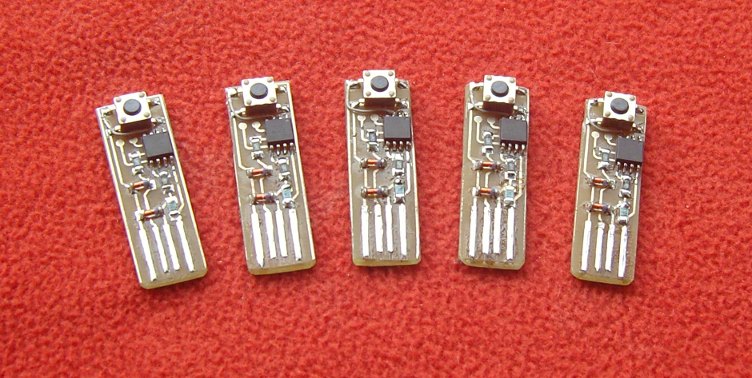
Here are the etched and tinned boards:
 |
| Etched and tinned playpause boards |
After tinning the boards, I cut them up using an abrasive wheel in my Dremel tool:
 |
| Etched, tinned and cut playpause boards, with artwork |
Then I file the edges of the boards, and give them a bevel. The boards are then ready for use.
So there you have it: PCBs from artwork to finished. I hope this is interesting and useful. Special thanks to Ross McK, who showed me how to do it. Ross is a great guy and a fine engineer, and he has taught me a lot.
Coming next: Playpause assembly and programming
Update: Here's
another very interesting page where the author also adds a solder-stop mask. His German heritage really shows, as his boards are wonderful!